- 您现在的位置:买卖IC网 > Sheet目录345 > MT42L256M32D4KP-3 IT:A (Micron Technology Inc)IC LPDDR2 SDRAM 8GBIT 168FBGA
�� �
�
�2Gb:� x16,� x32� Mobile� LPDDR2� SDRAM� S4�
�MODE� REGISTER� READ�
�MODE� REGISTER� READ�
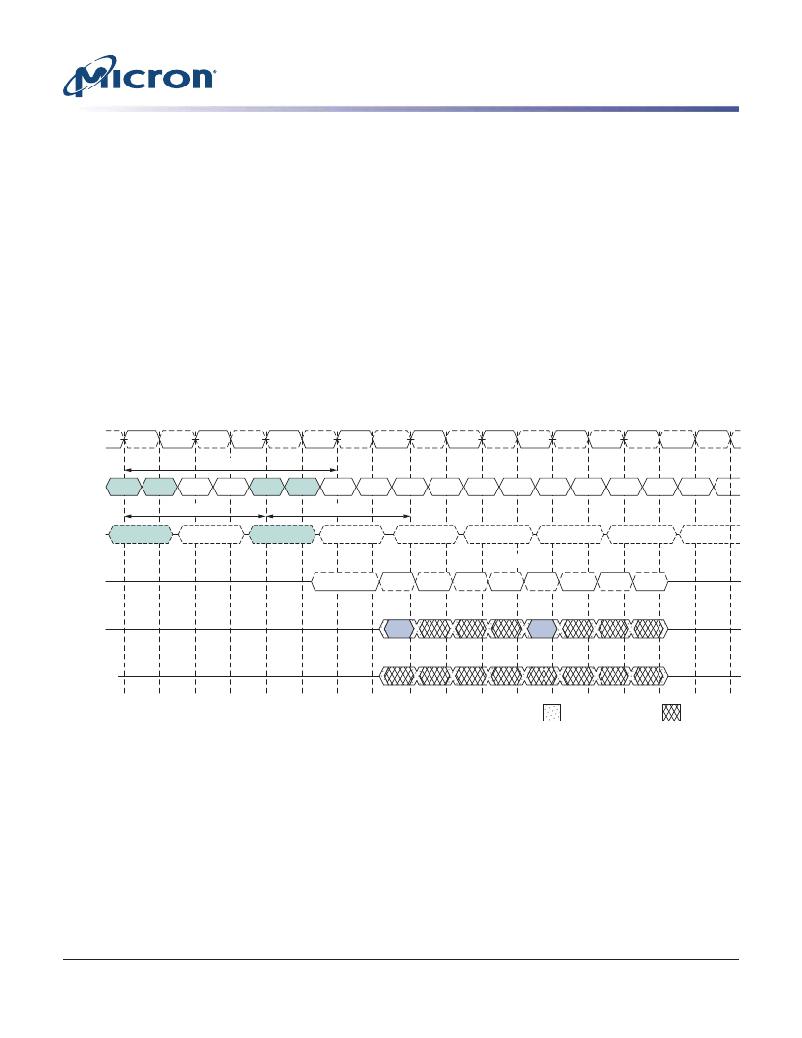
�The� MODE� REGISTER� READ� (MRR)� command� is� used� to� read� configuration� and� status�
�data� from� SDRAM� mode� registers.� The� MRR� command� is� initiated� with� CS#� LOW,� CA0�
�LOW,� CA1� LOW,� CA2� LOW,� and� CA3� HIGH� at� the� rising� edge� of� the� clock.� The� mode� reg-�
�ister� is� selected� by� CA1f–CA0f� and� CA9r–CA4r.� The� mode� register� contents� are� available�
�on� the� first� data� beat� of� DQ[7:0]� after� RL� � t� CK� +� t� DQSCK� +� t� DQSQ� and� following� the� ris-�
�ing� edge� of� the� clock� where� MRR� is� issued.� Subsequent� data� beats� contain� valid� but� un-�
�defined� content,� except� in� the� case� of� the� DQ� calibration� function,� where� subsequent�
�data� beats� contain� valid� content� as� described� in� Table� 47� (page� 90).� All� DQS� are� tog-�
�gled� for� the� duration� of� the� mode� register� READ� burst.�
�The� MRR� command� has� a� burst� length� of� four.� MRR� operation� (consisting� of� the� MRR�
�command� and� the� corresponding� data� traffic)� must� not� be� interrupted.� The� MRR� com-�
�mand� period� (� t� MRR)� is� two� clock� cycles.�
�Figure� 61:� MRR� Timing� –� RL� =� 3,� t� MRR� =� 2�
�T0�
�T1�
�T2�
�T3�
�T4�
�T5�
�T6�
�T7�
�T8�
�CK#�
�CK�
�RL� =� 3�
�CA[9:0]�
�Register� Register�
�A� A�
�Register� Register�
�B� B�
�t� MRR�
�=2�
�t� MRR�
�=2�
�CMD�
�MRR� 1�
�NOP� 2�
�MRR� 1�
�NOP� 2�
�Valid�
�DQS#�
�DQS�
�DQ[7:0]� 3�
�DQ[MAX:8]�
�D� OUT� A�
�D� OUT� B�
�Transitioning� data�
�Undefined�
�Notes:�
�1.� MRRs� to� DQ� calibration� registers� MR32� and� MR40� are� described� in� DQ� Calibration�
�(page� 89).�
�2.� Only� the� NOP� command� is� supported� during� t� MRR.�
�3.� Mode� register� data� is� valid� only� on� DQ[7:0]� on� the� first� beat.� Subsequent� beats� contain�
�valid� but� undefined� data.� DQ[MAX:8]� contain� valid� but� undefined� data� for� the� duration�
�of� the� MRR� burst.�
�4.� Minimum� MRR� to� write� latency� is� RL� +� RU(� t� DQSCKmax/� t� CK)� +� 4/2� +� 1� -� WL� clock� cycles.�
�5.� Minimum� MRR� to� MRW� latency� is� RL� +� RU(� t� DQSCKmax/� t� CK)� +� 4/2� +� 1� clock� cycles.�
�READ� bursts� and� WRITE� bursts� cannot� be� truncated� by� MRR.� Following� a� READ� com-�
�mand,� the� MRR� command� must� not� be� issued� before� BL/2� clock� cycles� have� completed.�
�Following� a� WRITE� command,� the� MRR� command� must� not� be� issued� before� WL� +� 1� +�
�BL/2� +� RU(� t� WTR/� t� CK)� clock� cycles� have� completed.� If� a� READ� or� WRITE� burst� is� trunca-�
�PDF:� 09005aef83f3f2eb�
�2gb_mobile_lpddr2_s4_g69a.pdf� –� Rev.� N� 3/12� EN�
�85�
�Micron� Technology,� Inc.� reserves� the� right� to� change� products� or� specifications� without� notice.�
�2010� Micron� Technology,� Inc.� All� rights� reserved.�
�发布紧急采购,3分钟左右您将得到回复。
相关PDF资料
MT45W1MW16BDGB-708 AT
IC PSRAM 16MBIT 104MHZ 54VFBGA
MT48H32M16LFB4-75B IT:C
IC SDRAM 512MB 54VFBGA
MT48H8M16LFB4-75 IT:K TR
IC SDRAM 128MBIT 133MHZ 54VFBGA
MTC100-JA2-P34
CONTACT INSERT PIN
MX841BE
IC CONVERTER WHITE LED 8-SOIC
MXHV9910BTR
IC LED DRIVER HIGH BRIGHT 8-SOIC
MXN12FB12F
MOTOR BRUSHED DC 12V 2922RPM
MXN13FB08B1
MOTOR BRUSHED DC 8V 4714RPM
相关代理商/技术参数
MT42L256M32D4KP-MS
制造商:Micron Technology Inc 功能描述:256MX32 LPDDR2 PLASTIC IND TEMP GREEN WFBGA 1.2V - Bulk